- 您现在的位置:买卖IC网 > Sheet目录3873 > PIC16CR76-I/ML (Microchip Technology)IC PIC MCU 8KX14 28QFN
PIC16CR7X
DS21993C-page 10
2007 Microchip Technology Inc.
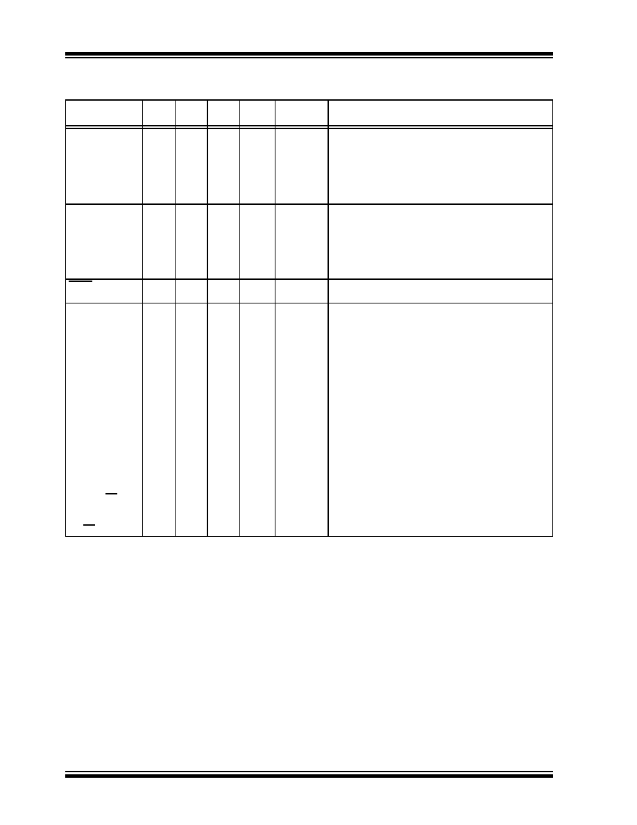
TABLE 1-3:
PIC16CR74 AND PIC16CR77 PINOUT DESCRIPTION
Pin Name
PDIP
Pin#
PLCC
Pin#
QFP
Pin#
I/O/P
Type
Buffer
Type
Description
OSC1/CLKIN
OSC1
CLKIN
13
14
30
I
ST/CMOS(4) Oscillator crystal or external clock input.
Oscillator crystal input or external clock source input.
ST buffer when configured in RC mode. Otherwise
CMOS.
External clock source input. Always associated with pin
function OSC1 (see OSC1/CLKIN, OSC2/CLKOUT
pins).
OSC2/CLKOUT
OSC2
CLKOUT
14
15
31
O
—
Oscillator crystal or clock output.
Oscillator crystal output.
Connects to crystal or resonator in Crystal Oscillator
mode.
In RC mode, OSC2 pin outputs CLKOUT, which has 1/4
the frequency of OSC1 and denotes the instruction
cycle rate.
MCLR
1
2
18
I
ST
Master Clear (Reset) input. This pin is an active low
Reset to the device.
PORTA is a bidirectional I/O port.
RA0/AN0
RA0
AN0
23
19
I/O
I
TTL
Digital I/O.
Analog input 0.
RA1/AN1
RA1
AN1
34
20
I/O
I
TTL
Digital I/O.
Analog input 1.
RA2/AN2
RA2
AN2
45
21
I/O
I
TTL
Digital I/O.
Analog input 2.
RA3/AN3/VREF
RA3
AN3
VREF
56
22
I/O
I
TTL
Digital I/O.
Analog input 3.
A/D reference voltage input.
RA4/T0CKI
RA4
T0CKI
67
23
I/O
I
ST
Digital I/O – Open drain when configured as output.
Timer0 external clock input.
RA5/AN4/SS
RA5
AN4
SS
78
24
I/O
I
TTL
Digital I/O.
Analog input 4.
SPI slave select input.
Legend:
I = input
O = output
I/O = input/output
P = power
— = Not used
TTL = TTL input
ST = Schmitt Trigger input
Note
1:
This buffer is a Schmitt Trigger input when configured as an external interrupt.
2:
This buffer is a Schmitt Trigger input when used in Serial Verify mode.
3:
This buffer is a Schmitt Trigger input when configured as general purpose I/O and a TTL input when used in the Parallel
Slave Port mode (for interfacing to a microprocessor bus).
4:
This buffer is a Schmitt Trigger input when configured in RC Oscillator mode and a CMOS input otherwise.
发布紧急采购,3分钟左右您将得到回复。
相关PDF资料
PIC16CR74T-I/ML
IC PIC MCU 4KX14 44QFN
PIC16CR74-I/PT
IC PIC MCU 4KX14 44TQFP
PIC16CR74-I/P
IC PIC MCU 4KX14 40DIP
PIC16CR74-I/ML
IC PIC MCU 4KX14 44QFN
PIC16CR73T-I/SS
IC PIC MCU 4KX14 28SSOP
PIC16CR73T-I/SO
IC PIC MCU 4KX14 28SOIC
PIC16CR73T-I/ML
IC PIC MCU 4KX14 28QFN
PIC16CR73-I/SS
IC PIC MCU 4KX14 28SSOP
相关代理商/技术参数
PIC16CR76-I/SO
功能描述:IC PIC MCU 8KX14 28SOIC RoHS:是 类别:集成电路 (IC) >> 嵌入式 - 微控制器, 系列:PIC® 16C 产品培训模块:XLP Deep Sleep Mode
8-bit PIC® Microcontroller Portfolio 标准包装:22 系列:PIC® XLP™ 18F 核心处理器:PIC 芯体尺寸:8-位 速度:48MHz 连通性:I²C,SPI,UART/USART,USB 外围设备:欠压检测/复位,POR,PWM,WDT 输入/输出数:14 程序存储器容量:8KB(4K x 16) 程序存储器类型:闪存 EEPROM 大小:256 x 8 RAM 容量:512 x 8 电压 - 电源 (Vcc/Vdd):1.8 V ~ 5.5 V 数据转换器:A/D 11x10b 振荡器型:内部 工作温度:-40°C ~ 85°C 封装/外壳:20-DIP(0.300",7.62mm) 包装:管件 产品目录页面:642 (CN2011-ZH PDF) 配用:DV164126-ND - KIT DEVELOPMENT USB W/PICKIT 2DM164127-ND - KIT DEVELOPMENT USB 18F14/13K50AC164112-ND - VOLTAGE LIMITER MPLAB ICD2 VPP
PIC16CR76-I/SP
功能描述:IC PIC MCU 8KX14 28DIP RoHS:是 类别:集成电路 (IC) >> 嵌入式 - 微控制器, 系列:PIC® 16C 产品培训模块:XLP Deep Sleep Mode
8-bit PIC® Microcontroller Portfolio 标准包装:22 系列:PIC® XLP™ 18F 核心处理器:PIC 芯体尺寸:8-位 速度:48MHz 连通性:I²C,SPI,UART/USART,USB 外围设备:欠压检测/复位,POR,PWM,WDT 输入/输出数:14 程序存储器容量:8KB(4K x 16) 程序存储器类型:闪存 EEPROM 大小:256 x 8 RAM 容量:512 x 8 电压 - 电源 (Vcc/Vdd):1.8 V ~ 5.5 V 数据转换器:A/D 11x10b 振荡器型:内部 工作温度:-40°C ~ 85°C 封装/外壳:20-DIP(0.300",7.62mm) 包装:管件 产品目录页面:642 (CN2011-ZH PDF) 配用:DV164126-ND - KIT DEVELOPMENT USB W/PICKIT 2DM164127-ND - KIT DEVELOPMENT USB 18F14/13K50AC164112-ND - VOLTAGE LIMITER MPLAB ICD2 VPP
PIC16CR76-I/SS
功能描述:IC PIC MCU 8KX14 28SSOP RoHS:是 类别:集成电路 (IC) >> 嵌入式 - 微控制器, 系列:PIC® 16C 产品培训模块:XLP Deep Sleep Mode
8-bit PIC® Microcontroller Portfolio 标准包装:22 系列:PIC® XLP™ 18F 核心处理器:PIC 芯体尺寸:8-位 速度:48MHz 连通性:I²C,SPI,UART/USART,USB 外围设备:欠压检测/复位,POR,PWM,WDT 输入/输出数:14 程序存储器容量:8KB(4K x 16) 程序存储器类型:闪存 EEPROM 大小:256 x 8 RAM 容量:512 x 8 电压 - 电源 (Vcc/Vdd):1.8 V ~ 5.5 V 数据转换器:A/D 11x10b 振荡器型:内部 工作温度:-40°C ~ 85°C 封装/外壳:20-DIP(0.300",7.62mm) 包装:管件 产品目录页面:642 (CN2011-ZH PDF) 配用:DV164126-ND - KIT DEVELOPMENT USB W/PICKIT 2DM164127-ND - KIT DEVELOPMENT USB 18F14/13K50AC164112-ND - VOLTAGE LIMITER MPLAB ICD2 VPP
PIC16CR76T-I/ML
功能描述:IC PIC MCU 8KX14 28QFN RoHS:是 类别:集成电路 (IC) >> 嵌入式 - 微控制器, 系列:PIC® 16C 产品培训模块:XLP Deep Sleep Mode
8-bit PIC® Microcontroller Portfolio 标准包装:22 系列:PIC® XLP™ 18F 核心处理器:PIC 芯体尺寸:8-位 速度:48MHz 连通性:I²C,SPI,UART/USART,USB 外围设备:欠压检测/复位,POR,PWM,WDT 输入/输出数:14 程序存储器容量:8KB(4K x 16) 程序存储器类型:闪存 EEPROM 大小:256 x 8 RAM 容量:512 x 8 电压 - 电源 (Vcc/Vdd):1.8 V ~ 5.5 V 数据转换器:A/D 11x10b 振荡器型:内部 工作温度:-40°C ~ 85°C 封装/外壳:20-DIP(0.300",7.62mm) 包装:管件 产品目录页面:642 (CN2011-ZH PDF) 配用:DV164126-ND - KIT DEVELOPMENT USB W/PICKIT 2DM164127-ND - KIT DEVELOPMENT USB 18F14/13K50AC164112-ND - VOLTAGE LIMITER MPLAB ICD2 VPP
PIC16CR76T-I/SO
功能描述:IC PIC MCU 8KX14 28SOIC RoHS:是 类别:集成电路 (IC) >> 嵌入式 - 微控制器, 系列:PIC® 16C 产品培训模块:XLP Deep Sleep Mode
8-bit PIC® Microcontroller Portfolio 标准包装:22 系列:PIC® XLP™ 18F 核心处理器:PIC 芯体尺寸:8-位 速度:48MHz 连通性:I²C,SPI,UART/USART,USB 外围设备:欠压检测/复位,POR,PWM,WDT 输入/输出数:14 程序存储器容量:8KB(4K x 16) 程序存储器类型:闪存 EEPROM 大小:256 x 8 RAM 容量:512 x 8 电压 - 电源 (Vcc/Vdd):1.8 V ~ 5.5 V 数据转换器:A/D 11x10b 振荡器型:内部 工作温度:-40°C ~ 85°C 封装/外壳:20-DIP(0.300",7.62mm) 包装:管件 产品目录页面:642 (CN2011-ZH PDF) 配用:DV164126-ND - KIT DEVELOPMENT USB W/PICKIT 2DM164127-ND - KIT DEVELOPMENT USB 18F14/13K50AC164112-ND - VOLTAGE LIMITER MPLAB ICD2 VPP
PIC16CR76T-I/SS
功能描述:IC PIC MCU 8KX14 28SSOP RoHS:是 类别:集成电路 (IC) >> 嵌入式 - 微控制器, 系列:PIC® 16C 产品培训模块:Asynchronous Stimulus
8-bit PIC® Microcontroller Portfolio 标准包装:42 系列:PIC® 16C 核心处理器:PIC 芯体尺寸:8-位 速度:20MHz 连通性:- 外围设备:欠压检测/复位,POR,PWM,WDT 输入/输出数:13 程序存储器容量:3.5KB(2K x 14) 程序存储器类型:OTP EEPROM 大小:- RAM 容量:128 x 8 电压 - 电源 (Vcc/Vdd):4 V ~ 5.5 V 数据转换器:A/D 4x8b 振荡器型:外部 工作温度:-40°C ~ 85°C 封装/外壳:18-SOIC(0.295",7.50mm 宽) 包装:管件 配用:XLT18SO-1-ND - SOCKET TRANSITION 18SOIC 300MILISPICR1-ND - ADAPTER IN-CIRCUIT PROGRAMMING309-1011-ND - ADAPTER 18-SOIC TO 18-DIP309-1010-ND - ADAPTER 18-SOIC TO 18-DIPAC164010-ND - MODULE SKT PROMATEII DIP/SOIC
PIC16CR77-I/ML
功能描述:IC PIC MCU 8KX14 44QFN RoHS:是 类别:集成电路 (IC) >> 嵌入式 - 微控制器, 系列:PIC® 16C 产品培训模块:Asynchronous Stimulus
8-bit PIC® Microcontroller Portfolio 标准包装:42 系列:PIC® 16C 核心处理器:PIC 芯体尺寸:8-位 速度:20MHz 连通性:- 外围设备:欠压检测/复位,POR,PWM,WDT 输入/输出数:13 程序存储器容量:3.5KB(2K x 14) 程序存储器类型:OTP EEPROM 大小:- RAM 容量:128 x 8 电压 - 电源 (Vcc/Vdd):4 V ~ 5.5 V 数据转换器:A/D 4x8b 振荡器型:外部 工作温度:-40°C ~ 85°C 封装/外壳:18-SOIC(0.295",7.50mm 宽) 包装:管件 配用:XLT18SO-1-ND - SOCKET TRANSITION 18SOIC 300MILISPICR1-ND - ADAPTER IN-CIRCUIT PROGRAMMING309-1011-ND - ADAPTER 18-SOIC TO 18-DIP309-1010-ND - ADAPTER 18-SOIC TO 18-DIPAC164010-ND - MODULE SKT PROMATEII DIP/SOIC
PIC16CR77-I/P
功能描述:IC PIC MCU 8KX14 40DIP RoHS:是 类别:集成电路 (IC) >> 嵌入式 - 微控制器, 系列:PIC® 16C 产品培训模块:Asynchronous Stimulus
8-bit PIC® Microcontroller Portfolio 标准包装:42 系列:PIC® 16C 核心处理器:PIC 芯体尺寸:8-位 速度:20MHz 连通性:- 外围设备:欠压检测/复位,POR,PWM,WDT 输入/输出数:13 程序存储器容量:3.5KB(2K x 14) 程序存储器类型:OTP EEPROM 大小:- RAM 容量:128 x 8 电压 - 电源 (Vcc/Vdd):4 V ~ 5.5 V 数据转换器:A/D 4x8b 振荡器型:外部 工作温度:-40°C ~ 85°C 封装/外壳:18-SOIC(0.295",7.50mm 宽) 包装:管件 配用:XLT18SO-1-ND - SOCKET TRANSITION 18SOIC 300MILISPICR1-ND - ADAPTER IN-CIRCUIT PROGRAMMING309-1011-ND - ADAPTER 18-SOIC TO 18-DIP309-1010-ND - ADAPTER 18-SOIC TO 18-DIPAC164010-ND - MODULE SKT PROMATEII DIP/SOIC